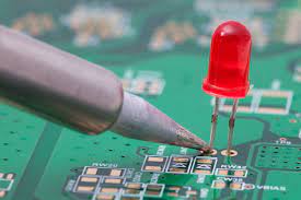
PCB fabrication is the process of creating these intricate, multi-layered boards that house the electronic components, enabling seamless communication and functionality. In the world of pcb assembly , precision is paramount, and this article delves into the intricacies of PCB fabrication.
The journey of PCB fabrication starts with a design phase, where engineers create a blueprint for the board, specifying the placement and routing of components. This design is then translated into a digital file using specialized software, which forms the basis for the PCB fabrication process.
The heart of PCB fabrication is the substrate, typically made of fiberglass-reinforced epoxy resin. This substrate acts as the supporting structure for the conductive pathways, providing both strength and insulation. Copper foil is bonded to the substrate, and a chemical etching process is employed to remove excess copper, leaving behind the desired circuit traces.
In multilayer PCBs, multiple copper-clad substrates are stacked and interconnected through vias, tiny holes that facilitate electrical connections between different layers. This intricate layering allows for more complex and compact circuit designs. To protect the exposed copper traces from environmental factors and to provide an additional layer of insulation, a solder mask is applied. This solder mask is typically green, but it can come in various colors.